Curing
The Photonic Curing Revolution:
High-temperature processing on low-temperature materials
Published – 6/14/2022
Author – Kurt A. Schroder, Ph.D
Engineered for industrial applications, while benefiting lab-scale R&D
While lasers can be used for sintering, they have poor quantum efficiency, small beam areas, only emit at one wavelength (which a given material might not absorb), and are expensive. A flashlamp, on the other hand, could theoretically be extremely fast, illuminate a large area, use broadband radiation that interacts with a huge array of materials, and are relatively inexpensive. But a flashlamp had never been engineered for the industrial applications we had in mind. So, we created the PulseForge, so called because it uses pulses of light to forge new materials.
To use a flashlamp effectively for sintering, one needs extremely precise control over the pulse length and even the pulse shape—that is, the intensity over time. Since a traditional flashlamp is driven by a simple pulse forming network (PFN), that means that one is generally limited to a single pulse length — and you can’t change the shape at all! The PulseForge® solves this issue by replacing the conventional Silicon Controlled Rectifier (SCR) based power system with an Insulated Gate Barrier Transistor (IGBT) based one. This innovation created a novel digital power delivery system that can deliver any pulse length or shape, increasing the number of process variables from 2 to over a dozen! By leveraging our company’s expertise in pulsed power, we were able to increase the peak power of our new flashlamp tool by a factor of 10 over a traditional flashlamp. This enabled dozens of thermal processes never before imagined on many different types of substrates including paper, plastic, glass, ceramics and even silicon!
Virtual photonic curing experiments

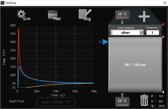
Figure 1. SimPulse simulation of 1 J/cm2 deposited on 1-micron thick Ag layer on 150-micron PET in 480 microseconds.
The PulseForge Invent is the result of many generations of design on our innovative flashlamp system, scaled down for use in a lab-scale R&D environment. The Invent uses the same components as our industrial tools, but in a smaller format. In addition to the precise pulse controls and integrated SimPulse environment, it has a synchronized linear motorized stage that can be used for large area curing or to replicate roll-to-roll processing. Depending on the configuration, it can have up to 4MW in the beam! The Invent is a modular R&D platform that can be upgraded as desired. It has an extensive suite of accessories which aid in processing, and the processing conditions can be easily exported to an industrial PulseForge. This means that scale up can be as simple as a few mouse clicks.
As one might guess, the technology behind the PulseForge has opened up dozens of applications beyond sintering. In the last ten years, over 100 patents have been issued on this technology and its applications. In the July installment of our series, we will share on the more advanced applications of photonic curing.

Kurt A. Schroder
Ph.D., CTO, PulseForge Inc
Related PulseForge in Research
Published – 6/14/2022
Author – Kurt A. Schroder, Ph.D
Download as a PDF
Engineered for industrial applications, while benefiting R&D
While lasers can be used for sintering, they have poor quantum efficiency, small beam areas, only emit at one wavelength (which a given material might not absorb), and are expensive. A flashlamp, on the other hand, could theoretically be extremely fast, illuminate a large area, use broadband radiation that interacts with a huge array of materials, and are relatively inexpensive. But a flashlamp had never been engineered for the industrial applications we had in mind. So, we created the PulseForge, so called because it uses pulses of light to forge new materials.
To use a flashlamp effectively for sintering, one needs extremely precise control over the pulse length and even the pulse shape—that is, the intensity over time. Since a traditional flashlamp is driven by a simple pulse forming network (PFN), that means that one is generally limited to a single pulse length — and you can’t change the shape at all! The PulseForge solves this issue by replacing the conventional Silicon Controlled Rectifier (SCR) based power system with an Insulated Gate Barrier Transistor (IGBT) based one. This innovation created a novel digital power delivery system that can deliver any pulse length or shape, increasing the number of process variables from 2 to over a dozen! By leveraging our company’s expertise in pulsed power, we were able to increase the peak power of our new flashlamp tool by a factor of 10 over a traditional flashlamp. This enabled dozens of thermal processes never before imagined on many different types of substrates including paper, plastic, glass, ceramics and even silicon!
Virtual photonic curing experiments

Figure 1. SimPulse simulation of 1 J/cm2 deposited on 1-micron thick Ag layer on 150-micron PET in 480 microseconds.
The PulseForge Invent is the result of many generations of design on our innovative flashlamp system, scaled down for use in a lab-scale R&D environment. The Invent uses the same components as our industrial tools, but in a smaller format. In addition to the precise pulse controls and integrated SimPulse environment, it has a synchronized linear motorized stage that can be used for large area curing or to replicate roll-to-roll processing. Depending on the configuration, it can have up to 4MW in the beam! The Invent is a modular R&D platform that can be upgraded as desired. It has an extensive suite of accessories which aid in processing, and the processing conditions can be easily exported to an industrial PulseForge. This means that scale up can be as simple as a few mouse clicks.
As one might guess, the technology behind the PulseForge has opened up dozens of applications beyond sintering. In the last ten years, over 100 patents have been issued on this technology and its applications. In the July installment of our series, we will share on the more advanced applications of photonic curing.

Kurt A Schroder
Ph.D., CTO, PulseForge Inc