High throughput, low-stress, low-residue, room temperature debonding
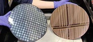
Suitable for wafer-level and panel-level packaging, PulseForge Photonic Debonding offers ash-free wafer separation with fewer contaminants and lower cost compared to lasers.
It can also be used on warped wafers without hardware or process changes. This is partly due to PulseForge not being a point source like lasers, but its beam is homogenous even at a 10 mm Z distance from the lamp. This makes the chip-embedded EMC wafers market (Fan-out packages) uniquely suitable for photonic debonding.
The process involves illuminating an intense pulse of light onto a very thin light-absorbing layer (LAL) through the glass substrate for a few hundred microseconds. The LAL absorbs the light, converting it very quickly to heat. This causes the interfacial adhesive layer to be instantaneously ablated. Ablation of the thin interfacial layer forms a thermally insulating layer (e.g. air) between the LAL and the remaining portions of the stack, creating an adhesion loss and protecting it from thermal stress. Finally, the wafer can be separated from the carrier with zero force. The carrier can be further cleaned and reused with a brand-new wafer, decreasing the cost of processing per wafer.

Lower TCO by 30% or more
Cleaner process – no ash or residue
Compatible with warped substrates
Modular design for ease of integration
Faster throughput: >100wph
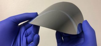
Thinned wafer (~50 μm)
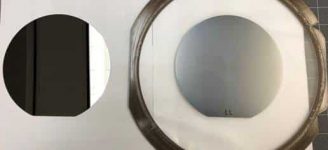
Thinned wafer debonding for 3D integration