

Lower TCO by 30% or more
Cleaner process – no ash or residue
Compatible with warped substrates
Configurable for different wafer sizes
Fully automated x-y stage
Minimum of 30% TCO Reduction
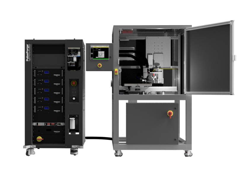
The PulseForge PD300 SA is a semi-automated system for debonding temporarily bonded wafer pairs. The PulseForge patented photonic debonding process utilizes a high-intensity flash lamp in conjunction with our proprietary, reusable light-absorbing layer carriers. The solution delivers a minimum 30% reduction in the total cost of ownership (TCO) and provides a clean, zero-force carrier separation.
Suitable for both wafer-level and panel-level packaging, the PD300 SA is ideal for low- volume and R&D applications. It can debond warped wafers without expensive warpage adjustment hardware or process changes. This makes the chip-embedded EMC wafers market (Fan-out packages) uniquely suitable for photonic debonding.
Features
- Complete automation of the stage movement and synchronization with flash lamp processing
- Storable process flow protocol
- Digitally adjustable process conditions
- Accommodates up to 300 mm wafers on tape frame
- Interchangeable fixtures allow quick reconfiguration for different wafer sizes
- Ability to debond panels of up to 400 mm x 400 mm
- Capable of processing up to 20 wafers per hour
- Secured and interlock- controlled light shielding
- Patented water cooling to prevent heat build- up
Specs and Supporting Information
Lower TCO by 30% or more
Cleaner process – no ash or residue
Compatible with warped substrates
Configurable for different wafer sizes
Fully automated x-y stage
Are you ready to discover the impact of photonic debonding?
