An introduction to a new application from PulseForge with guiding questions for collaborators and customers…
PulseForge continues to bring new technologies to the printed electronics market to enable new structures and patterns that were previously considered unfeasible, too costly or impossible to manufacture. In this blog post we introduce the reader to PulseForge® Printing, a novel new way for contactless printing of a wide range of materials. This technology uses the capabilities developed in the PulseForge light source to instantaneously heat an ink loaded in a patterned plate. On heating, the ink is ejected from the plate and onto a target substrate – transferring the pattern. Our patterned plate gives the printer the ability to make very high resolution (< 25 µm), high aspect ratio (~ 1 for a single print), and multi-height prints out of a wide range of materials. Our PulseForge tool set gives the process high throughput, high duty cycle, repeatability, and uniformity. Common initial questions are outlined in this post with our answers to initiate a discussion around what this technology is capable of. Please connect with our team to learn more and engage on specific projects that could benefit from the capabilities of our new PulseForge Printing application.
What is PulseForge Printing?
It is an emerging application from NovaCentrix for patterning high aspect ratio prints of a wide variety of functional inks or other materials and components in a rapid, non-contact technique. The printing is achieved using high power pulsed light and an engraved print plate. The images below show before (left) and after (right) the light pulse.
Compared with other non-contact printing techniques (particularly inkjet and aerosol jet printing), PulseForge Printing is compatible with a wide range of ink viscosities and well-suited for high viscosity formulations. For conductive ink, PulseForge Printing is well-suited for very high loading inks which enables additional functionality.

The next few questions will highlight some of the particular advantages of PulseForge Printing over other patterning techniques.
Can I produce a print with different thicknesses in one pattern?
Yes, by patterning a print plate, this process is compatible with multi-thickness patterning. This can be considered a 2.5D printing technology. Variable print thicknesses are shown in the illustration and microscope images below. There is an example contact pad and lead frame pattern where the pads are pillars at a greater thickness than the leads (printed copper).

The ability to print various thicknesses at once enables replacing multiple printing steps with a single PulseForge printing step.
Can multiple prints be aligned? Does registration work?
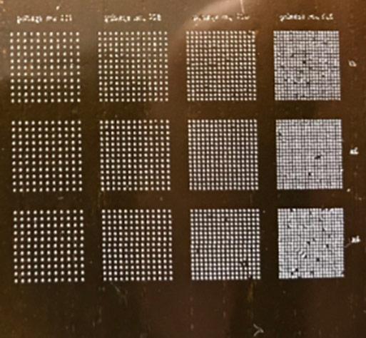
Yes, this technique is compatible with aligned printing and we have demonstrated this with a few different alignment methods. We are always interested to work with partners to integrate into their preferred alignment method. The microscope photo enlarged at the top of this document shows multiple aligned prints of copper ink on a glass substrate.
Current process capability enables resolution of < 25 µm with < 50 µm pitch. Aligned printing at such fine resolution requires more sophisticated overlay techniques than simple optical registration.
Can I print over gaps or non-flat surfaces?
Yes, as a non-contact printing technique, this is compatible with printing on non-flat surfaces and even over gaps. We have also demonstrated the ability to print and ‘swing-around’ an edge with silver conductive ink. The photos and microscope images below show silver ink printed on various substrates with gaps, around edges, and non-flat surfaces.

How thick can I print? What is the maximum aspect ratio?
Very thick prints (> 1.5 mm) are feasible. Utilizing aligned printing can also result in very high aspect ratio (> 2). For a single print from a single plate, the maximum aspect ratio is ~ 1. Note that high viscosity inks help to maintain a high aspect ratio print through drying and curing. The images below show topography of a v-shaped channel pattern giving a high aspect ratio. The plate pattern is shown at the right and the printed ink is at the left.

Can I print my own ink? What inks has NovaCentrix developed?
Yes, we have demonstrated the ability to print a wide range of materials because we have designed the print plates to absorb and heat locally due to the pulsed light. There is a wide range of materials that will volatilize and eject and print from our plates. The photo below shows an array of SAC305 solder paste in an array pattern printed onto a polyimide substrate.
NovaCentrix has developed several high viscosity (> 1 M cps) copper and silver inks for PulseForge printing applications, and as always custom formulations can be developed to meet customers’ requirements.

Can I print on light- or temperature-sensitive substrates? Are there other limitations regarding substrates?
As a non-contact printing technique, PulseForge Printing is compatible with almost any substrate. The main parameter to consider is adhesion between the ink and the substrate. The plate is designed such that the substrate is not exposed to the light pulse.
Does printing require a special PulseForge tool?
In short, yes, the printing process requires a short light pulse with high peak power (> 40 kW/cm2). A high voltage power supply PulseForge 1300, 3300 or Invent equivalent is capable to generate print pulses.

| Written by Harry ChouHarry Chou is an Application Engineer at NovaCentrix developing new processes with partners and customers, as well as building new technologies within the company. He tackles technical challenges systematically to ensure all collaborators have visibility into experimental plans and results. His collaborations extend beyond the NovaCentrix facility in Austin to companies and institutions all over. He is working to show how photonic processes and functional nanomaterials can impact a broad range of technologies. Harry’s industry experience includes startup and entrepreneurship ventures with novel nanomaterials, as well as in characterization and analysis with semiconductors. Harry has published and reviewed dozens of articles for scientific journals and holds a PhD in Materials Science and Engineering from the University of Texas at Austin where he researched synthesis, characterization, and applications of novel nanomaterials. He also holds a BS in Materials Science and Engineering from UC Berkeley. |
