Published – 7/11/2022
Author – Kurt A. Schroder, Ph.D
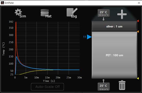
Figure 1. Simple pulse processing a thin nanoparticle silver layer on PET in 350 microseconds.
Consider a simple pulse of light irradiating a printed silver nanoparticle ink on top of a PET substrate in Figure 1. We wish to sinter the nanoparticles to form an electrically conductive trace. The flashlamp is turned on for 350 microseconds and rapidly heats the surface temperature of the silver trace briefly to 392 °C to render the printed trace electrically conductive. This is just below the gasification temperature of the PET substrate and nearly 250 °C higher than that which could be achieved by a traditional oven. This higher temperature capability is the principal reason why PulseForge technology regularly outperforms oven processing when processing functional films.
Still, if we could maintain that peak temperature longer, the silver nanoparticles would be sintered even more effectively, and the conductivity would be even higher! With a traditional flashlamp system, this is impossible, but with a digital flashlamp system, we can do this with a technique called “pulse shaping,” which is similar to pulse width modulation. Figure 2 shows how. Here, we rapidly turn the flashlamp on and off delivering multiple pulses with microsecond precision over a timescale of just a couple milliseconds. The benefits this imparts are not obvious, as it appears to be a random string of arbitrary length pulses. But with our machine-integrated thermal stack simulator, SimPulse®, we can visualize what is happening and engineer the timing of the pulse stream.
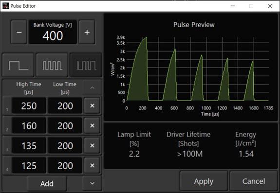
Figure 2. Full shaped pulse profile. Only the timing for the first 4 pulses is shown.
Figure 3 shows the results. With the precise timing of the pulses, we are effectively able to extend the pulse to maintain the peak temperature at the surface. But there are multiple items happening here. In addition to maintaining the peak temperature, the intentional pauses in the pulses allow time for gas to be ejected during processing. Additionally, the pauses in the pulse string also allow for just enough heat to soak into the substrate to reduce thermal stresses associated with differences in the coefficient of thermal expansion of different layers in the stack. In effect, it allows the film to be processed more deeply and faster without failing the film. Figure 4 shows that thermal equilibrium of the thin film stack is attained in only about 20ms after processing. Since very little energy is used to process the film, the temperature of the entire stack has only increased from 25 °C to 90 °C! In effect, the film has seen a high thermal budget, which increases the quality of the cure, but the substrate, which is the weak link in the system, has seen very little overall thermal budget. We can continue to add more pulses to the processing profile as long as the equilibration temperature does not exceed 150 °C.
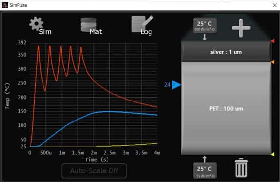
Figure 3. Response of thin film stack to engineered shaped pulse.
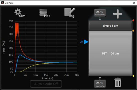
Figure 4. Thermal equilibrium of the thin film stack is reached ~20ms after processing. It has only been heated from 25 °C to 90 °C.

Kurt A. Schroder
Ph.D., CTO, PulseForge Inc
Related PulseForge in Research
Published – 7/11/2022
Author – Kurt A. Schroder, Ph.D
Download as a PDF

Figure 1. Simple pulse processing a thin nanoparticle silver layer on PET in 350 microseconds.
Consider a simple pulse of light irradiating a printed silver nanoparticle ink on top of a PET substrate in Figure 1. We wish to sinter the nanoparticles to form an electrically conductive trace. The flashlamp is turned on for 350 microseconds and rapidly heats the surface temperature of the silver trace briefly to 392 °C to render the printed trace electrically conductive. This is just below the gasification temperature of the PET substrate and nearly 250 °C higher than that which could be achieved by a traditional oven. This higher temperature capability is the principal reason why PulseForge technology regularly outperforms oven processing when processing functional films.
Still, if we could maintain that peak temperature longer, the silver nanoparticles would be sintered even more effectively, and the conductivity would be even higher! With a traditional flashlamp system, this is impossible, but with a digital flashlamp system, we can do this with a technique called “pulse shaping,” which is similar to pulse width modulation. Figure 2 shows how. Here, we rapidly turn the flashlamp on and off delivering multiple pulses with microsecond precision over a timescale of just a couple milliseconds. The benefits this imparts are not obvious, as it appears to be a random string of arbitrary length pulses. But with our machine-integrated thermal stack simulator, SimPulse®, we can visualize what is happening and engineer the timing of the pulse stream.

Figure 2. Full shaped pulse profile. Only the timing for the first 4 pulses is shown.
Figure 3 shows the results. With the precise timing of the pulses, we are effectively able to extend the pulse to maintain the peak temperature at the surface. But there are multiple items happening here. In addition to maintaining the peak temperature, the intentional pauses in the pulses allow time for gas to be ejected during processing. Additionally, the pauses in the pulse string also allow for just enough heat to soak into the substrate to reduce thermal stresses associated with differences in the coefficient of thermal expansion of different layers in the stack. In effect, it allows the film to be processed more deeply and faster without failing the film. Figure 4 shows that thermal equilibrium of the thin film stack is attained in only about 20ms after processing. Since very little energy is used to process the film, the temperature of the entire stack has only increased from 25 °C to 90 °C! In effect, the film has seen a high thermal budget, which increases the quality of the cure, but the substrate, which is the weak link in the system, has seen very little overall thermal budget. We can continue to add more pulses to the processing profile as long as the equilibration temperature does not exceed 150 °C.

Figure 3. Response of thin film stack to engineered shaped pulse.

Figure 4. Thermal equilibrium of the thin film stack is reached ~20ms after processing. It has only been heated from 25 °C to 90 °C.

Kurt A. Schroder
Ph.D., CTO, PulseForge Inc