PulseForge Ash-Free Debonding
Debonding in a Fraction of the Time, and Ash-Free
Published – 10/18/2022
Author – Vikram Turkani
As Moore’s law maintains its relentless march, devices continually become smaller, more powerful, more efficient, and more complex. Engineers are finding ways to pack more and more components into tinier spaces. These advances require clever packaging solutions to allow for handling and integration of packaged components. Two of the most watched next-generation packaging approaches are 3-dimensional integrated circuit (3DIC) and fan-out wafer-level packaging (FOWLP). Engineers at PulseForge, Inc. have recently developed an exciting new application for the PulseForge technology in FOWLP processing.
Today many of these packaging approaches involve processing thin wafers that must be mechanically supported during the manufacturing in order to mitigate the risk of breakage while handling. This is accomplished by having wafers mounted to a temporary carrier, bonded with a polymer adhesive. The carrier can then act as a rigid scaffold, protecting the fragile wafers from breaking apart. Then, after the devices are fully fabricated, the wafer must be removed from the carrier. This process is called temporary bonding/debonding (TB/DB).
|
Process Method
|
Thermal Stress
|
Mechanical Stress
|
Processing Time
|
Process Integration
|
Harsh Chemicals
|
Processing Cost
|
|---|---|---|---|---|---|---|
|
Chemical Debonding
|
Low
|
Low
|
Medium
|
Difficult
|
Yes
|
High
|
|
Mechanical Debonding
|
Low
|
High
|
Medium
|
Simple
|
No
|
Medium
|
|
Laser Debonding
|
Low-Medium
|
Low
|
Medium
|
Simple
|
No
|
Medium
|
|
Thermal Debonding
|
High
|
Medium
|
High
|
Difficult
|
No
|
High
|
|
PulseForge Debonding
|
Low
|
Low
|
Low
|
Simple
|
No
|
Low
|
Table of existing commercialized methods and their relative advantages and disadvantages.
Debonding Stack
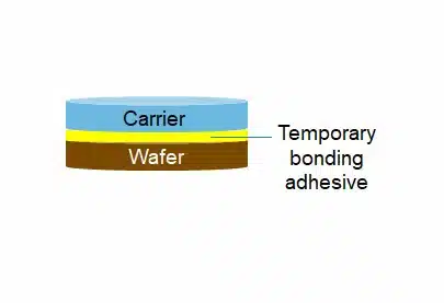
Chemical Debonding
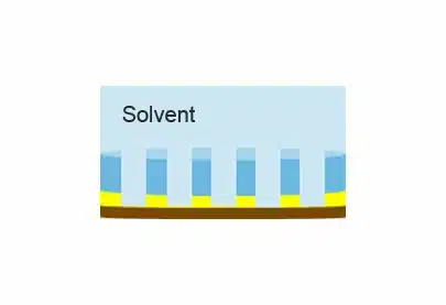
Mechanical Debonding
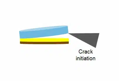
Laser Debonding
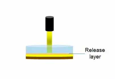
Thermal Debonding
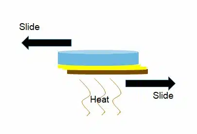
PulseForge Debonding
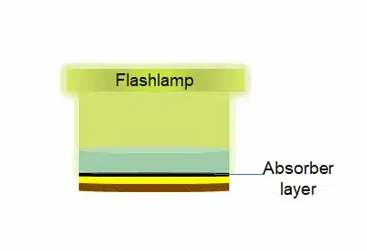
Figure 1. Various Types of Debonding Solutions.
Current TB/DB debonding steps are slow, expensive, and carry a high risk of destruction and contamination to the newly formed components. PulseForge TB/DB does not require any chemical solvents, as chemical debonding does, or the heating and cooling of an oven environment, as thermal debonding does. Additionally, it isn’t necessary to shear the wafer relative to the carrier to achieve debonding, as both these methods do. PulseForge debonding also does not require a constant supply of gas, as laser debonding systems do. Since the lamp illuminates around 100 cm2 at once, it can process a wafer an order of magnitude more quickly than a laser, whose illuminated area can be as low as around 1 cm2. The much simpler hardware of the PulseForge eliminates the cost of labor to align and maintain the laser optics involved with laser debonding as well.
PulseForge debonding was developed to circumvent these issues and provide a better solution. First, a very thin metal light-absorbing layer is applied to the glass carrier before the adhesive layer is deposited. After the wafer is mounted to the carrier and formed into the desired devices, the glass carrier is exposed to the PulseForge flash lamp. The metal TiW layer absorbs that light, converting it very quickly to heat. That very intense, short-lived pulse causes the interfacial adhesive layer to be instantaneously ablated. Ablation of the thin interfacial layer forms a thermally insulating layer between the TiW light-absorbing layer and the remaining portions of the stack, protecting from thermal stress. Finally, the wafer can be easily separated from the carrier by gentle vacuum, and the carrier can be cleaned and reused with a brand-new wafer which further decreases the cost of processing per wafer.
Recently, wafer warpage has become a common issue in fan-out wafer level packaging. This is because materials with two different co-efficient of thermal expansion such as glass and epoxy-mold compound (EMC) are bonded together. PulseForge enables the debonding of wafers with warpage without any hardware or process changes. This is in part due to PulseForge not being a point source like lasers but its beam is homogenous even at 10 mm Z distance from the lamp. This makes the chip-embedded EMC wafers market (Fan-out packages) uniquely suitable for photonic debonding.
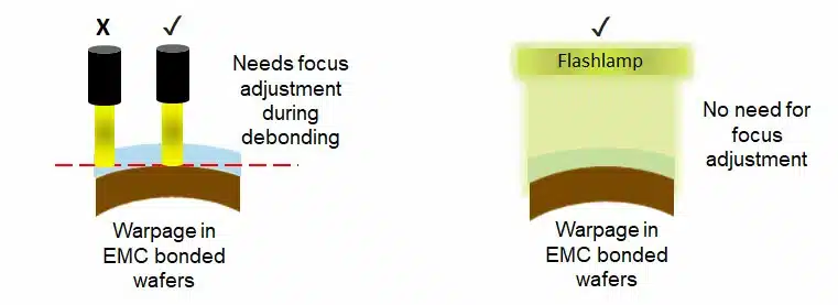
Figure 2. Wafer warpage
This TB/DB development relies on unique capabilities of the PulseForge technology. The PulseForge tools are designed to deliver short, high voltage electrical pulses to a noble gas flashlamp, which in turn radiates intense light pulses. The PulseForge lamp irradiates the sample with such intense broadband light that the temperature of the light-absorber in the light path can go up hundreds of degrees in a matter of microseconds. Our design team has devised modular housing for this innovative device, so that it can be easily integrated into existing TB/DB tools and process lines. We are currently working with semiconductor process integrators, like SUSS MicroTec, to incorporate this technology into their equipment for TB/DB.
Because of the ease of process integration, the low cost of ownership, and the fast process development that the PulseForge affords, it is a great technology for many manufacturing applications in addition to semiconductor manufacturing unit operations. Aside from TB/DB, it has been applied to soldering, display liftoff, and printing uses, where it offers faster, less expensive processing than many existing technologies. With a few minor process additions, the same benefits can be realized by the temporary bonding and debonding space. PulseForge, Inc. is currently seeking partnerships to join the design feedback loop and help bring PulseForge debonding out of the lab and into the fab.

Vikram Turkani,
Technical Program Manager,
PulseForge Inc
Related PulseForge In Research
Published – 10/18/2022
Author – Vikram Turkani
Download as a PDF
As Moore’s law maintains its relentless march, devices continually become smaller, more powerful, more efficient, and more complex. Engineers are finding ways to pack more and more components into tinier spaces. These advances require clever packaging solutions to allow for handling and integration of packaged components. Two of the most watched next-generation packaging approaches are 3-dimensional integrated circuit (3DIC) and fan-out wafer-level packaging (FOWLP). Engineers at PulseForge, Inc. have recently developed an exciting new application for the PulseForge technology in FOWLP processing.
Today many of these packaging approaches involve processing thin wafers that must be mechanically supported during the manufacturing in order to mitigate the risk of breakage while handling. This is accomplished by having wafers mounted to a temporary carrier, bonded with a polymer adhesive. The carrier can then act as a rigid scaffold, protecting the fragile wafers from breaking apart. Then, after the devices are fully fabricated, the wafer must be removed from the carrier. This process is called temporary bonding/debonding (TB/DB).
|
Process Method
|
Thermal Stress
|
Mechanical Stress
|
Processing Time
|
Process Integration
|
Harsh Chemicals
|
Processing Cost
|
|---|---|---|---|---|---|---|
|
Chemical Debonding
|
Low
|
Low
|
Medium
|
Difficult
|
Yes
|
High
|
|
Mechanical Debonding
|
Low
|
High
|
Medium
|
Simple
|
No
|
Medium
|
|
Laser Debonding
|
Low-Medium
|
Low
|
Medium
|
Simple
|
No
|
Medium
|
|
Thermal Debonding
|
High
|
Medium
|
High
|
Difficult
|
No
|
High
|
|
PulseForge Debonding
|
Low
|
Low
|
Low
|
Simple
|
No
|
Low
|
Table of existing commercialized methods and their relative advantages and disadvantages.
Debonding Stack

Chemical Debonding

Mechanical Debonding

Laser Debonding

Thermal Debonding

PulseForge Debonding

Figure 1. Various Types of Debonding Solutions.
Current TB/DB debonding steps are slow, expensive, and carry a high risk of destruction and contamination to the newly formed components. PulseForge TB/DB does not require any chemical solvents, as chemical debonding does, or the heating and cooling of an oven environment, as thermal debonding does. Additionally, it isn’t necessary to shear the wafer relative to the carrier to achieve debonding, as both these methods do. PulseForge debonding also does not require a constant supply of gas, as laser debonding systems do. Since the lamp illuminates around 100 cm2 at once, it can process a wafer an order of magnitude more quickly than a laser, whose illuminated area can be as low as around 1 cm2. The much simpler hardware of the PulseForge eliminates the cost of labor to align and maintain the laser optics involved with laser debonding as well.
PulseForge debonding was developed to circumvent these issues and provide a better solution. First, a very thin metal light-absorbing layer is applied to the glass carrier before the adhesive layer is deposited. After the wafer is mounted to the carrier and formed into the desired devices, the glass carrier is exposed to the PulseForge flash lamp. The metal TiW layer absorbs that light, converting it very quickly to heat. That very intense, short-lived pulse causes the interfacial adhesive layer to be instantaneously ablated. Ablation of the thin interfacial layer forms a thermally insulating layer between the TiW light-absorbing layer and the remaining portions of the stack, protecting from thermal stress. Finally, the wafer can be easily separated from the carrier by gentle vacuum, and the carrier can be cleaned and reused with a brand-new wafer which further decreases the cost of processing per wafer.
Recently, wafer warpage has become a common issue in fan-out wafer level packaging. This is because materials with two different co-efficient of thermal expansion such as glass and epoxy-mold compound (EMC) are bonded together. PulseForge enables the debonding of wafers with warpage without any hardware or process changes. This is in part due to PulseForge not being a point source like lasers but its beam is homogenous even at 10 mm Z distance from the lamp. This makes the chip-embedded EMC wafers market (Fan-out packages) uniquely suitable for photonic debonding.

Figure 2. Wafer warpage
This TB/DB development relies on unique capabilities of the PulseForge technology. The PulseForge tools are designed to deliver short, high voltage electrical pulses to a noble gas flashlamp, which in turn radiates intense light pulses. The PulseForge lamp irradiates the sample with such intense broadband light that the temperature of the light-absorber in the light path can go up hundreds of degrees in a matter of microseconds. Our design team has devised modular housing for this innovative device, so that it can be easily integrated into existing TB/DB tools and process lines. We are currently working with semiconductor process integrators, like SUSS MicroTec, to incorporate this technology into their equipment for TB/DB.
Because of the ease of process integration, the low cost of ownership, and the fast process development that the PulseForge affords, it is a great technology for many manufacturing applications in addition to semiconductor manufacturing unit operations. Aside from TB/DB, it has been applied to soldering, display liftoff, and printing uses, where it offers faster, less expensive processing than many existing technologies. With a few minor process additions, the same benefits can be realized by the temporary bonding and debonding space. PulseForge, Inc. is currently seeking partnerships to join the design feedback loop and help bring PulseForge debonding out of the lab and into the fab.

Vikram Turkani
Technical Program Manager, PulseForge Inc