Semiconductor Processing Without Ash or Chemicals.
Be at the cutting edge with PulseForge Photonic Debonding
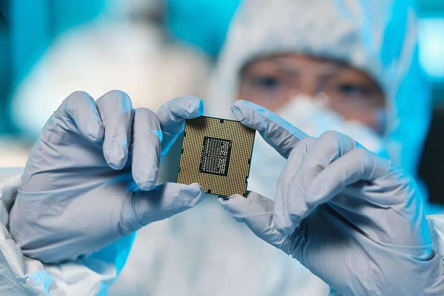
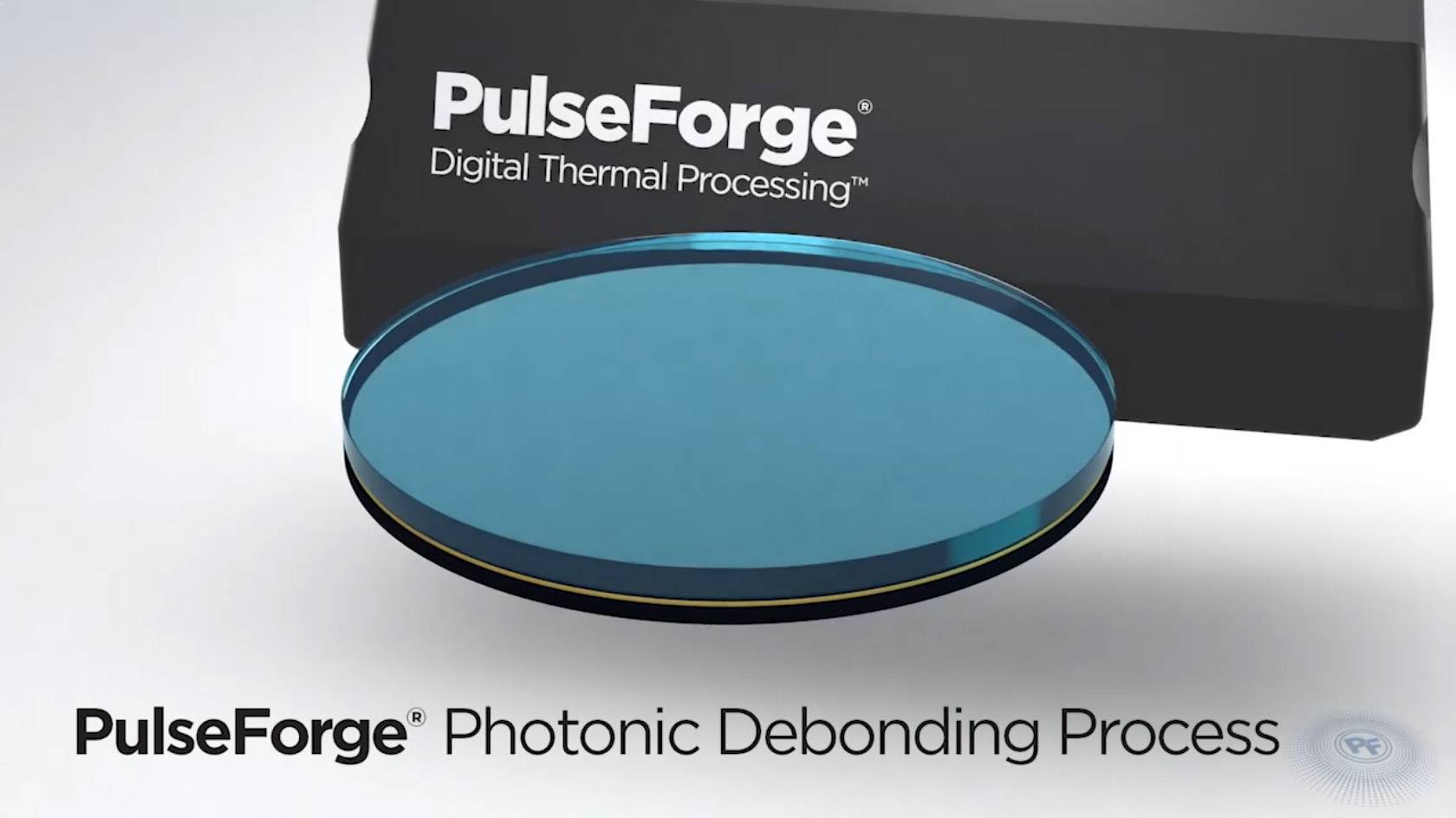
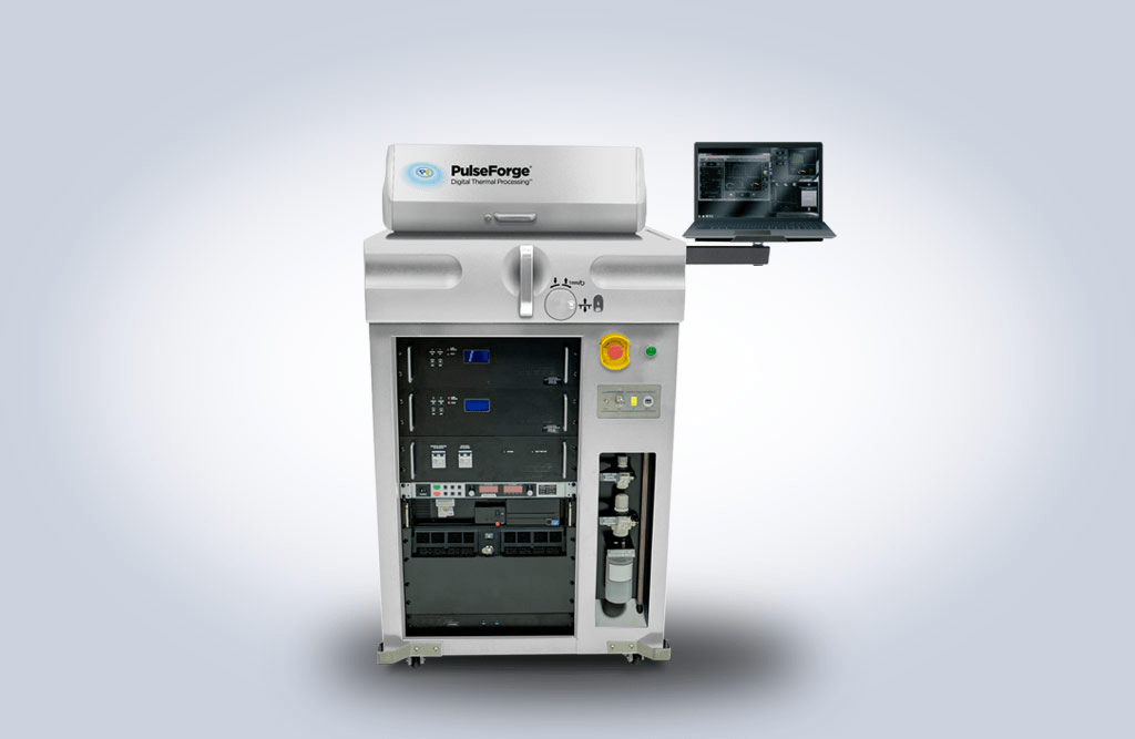
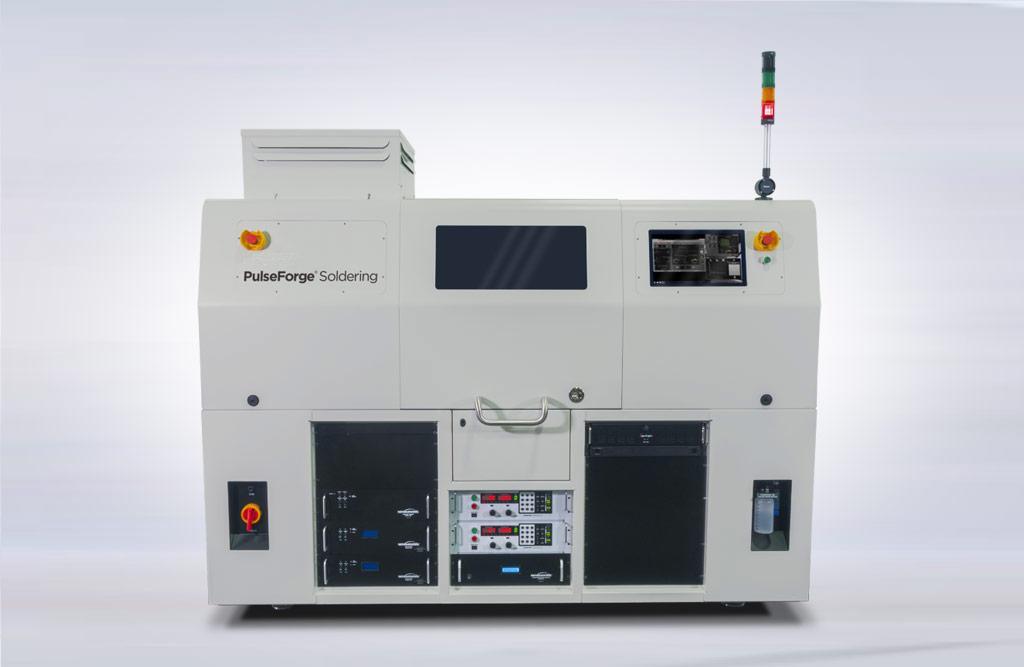
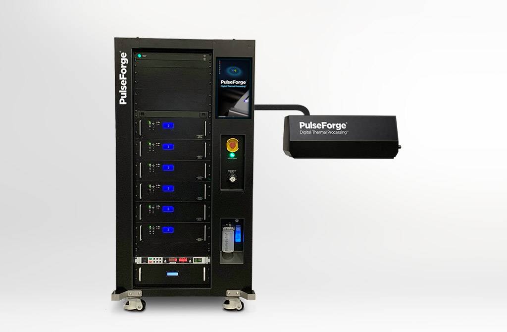
The drive for Moore’s Law is relentless. New technologies throughout the semiconductor manufacturing cycle have to be the answer, and PulseForge delivers. Our debonding technology offers ash-free wafer separation with fewer contaminants and lower costs compared to lasers. Photonic Debonding is also uniquely suited for chip-embedded EMC wafers (fan-out packages) as we are able to debond warped wafers without any hardware or process changes. Our soldering tools offer on-wafer bumping at a fraction of the time and thermal budget so sensitive architectures don’t get damaged. Plus, explore our tools for unique cleaning solutions for ultra-fine-pitch features, dehydrogenation, and even novel TFT designs.
