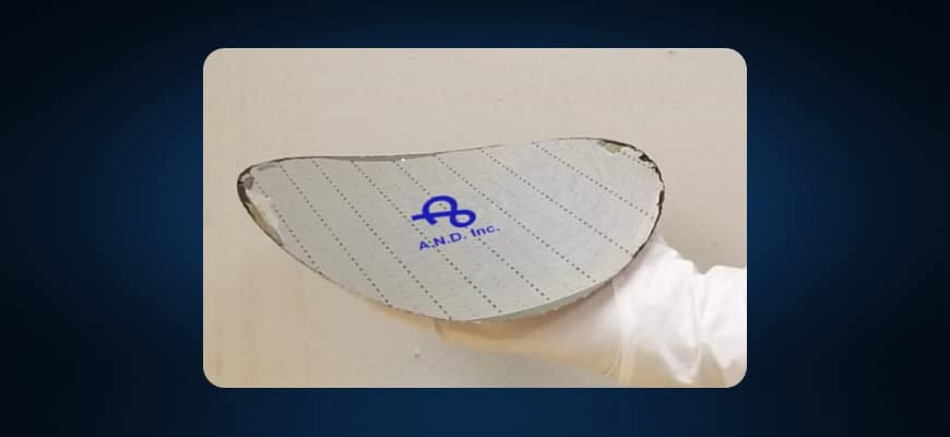
Austin, Texas – August 29, 2023 – PulseForge Inc., a recognized leader in applied thermal energy, and Applied Novel Devices (AND), a pioneering force in new semiconductor device architectures for discrete and integrated power products, have joined forces to demonstrate a groundbreaking advancement in the field of power electronics packaging through photonic debonding. This collaborative effort aims to revolutionize power electronics manufacturing by enhancing efficiency, reducing costs, and enabling high-performance packaging solutions.
This partnership involved testing AND’s state-of-the-art power MOSFET wafers with PFI’s photonic debonding process. These wafers were temporarily bonded to PFI’s reusable inorganic light absorbing layer-coated glass carrier and debonded using PFI’s photonic debonding PD- 300 SA tool. Post cleaning, all the MOSFETs demonstrated the same performance as they did before going through a temporary bonding and debonding process.
The accomplishment of a 100% yield is a testament to the innovative photonic debonding process, which has set a course to redefine electronics packaging with its unmatched throughput, cleaner debond without any ash-residue, and lower cost of ownership.
“We are thrilled to celebrate this remarkable achievement alongside Applied Novel Devices,” stated Jonathan Gibson, CEO of PulseForge. “This accomplishment not only demonstrates the power of collaboration, but also the immense possibilities that photonic debonding holds for the future of power electronics packaging.”
Both PulseForge and Applied Novel Devices teams recognize the profound significance of this collaboration. They remain steadfast in their commitment to disseminate the technical intricacies to prospective customers keen on exploring the potential of photonic debonding in conjunction with AND’s pioneering and highly efficient power MOSFETs, especially in the growing power devices market.
“PulseForge has demonstrated a scalable path to overcome throughput and cost challenges of current wafer debonding technologies. AND is excited to work with PulseForge in bringing this technology to volume production” said Leo Mathew, CEO of Applied Novel Devices.
About PulseForge, Inc.
PulseForge utilizes applied energy in a precise and targeted manner to enable innovation in industrial manufacturing. Our expertise and tools empower our customers to explore novel materials and manufacturing methodologies, driving dynamic and efficient production at an industrial scale.
About Applied Novel Devices
Applied Novel Devices (AND) is based in Austin, Texas. AND develops new semiconductor device architectures that address the next generation of applications using its novel process technologies for discrete and integrated power products. AND has developed the tools and technologies for thin-crystalline semiconductor devices and has targeted power MOSFETs for this technology.
