Argonne and PulseForge Advance Solid-State Electrolyte Manufacturing in Phase 2 CRADA
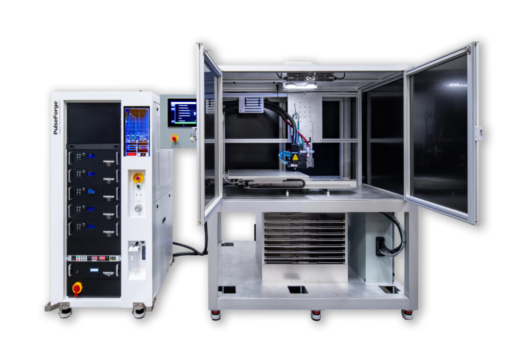
PulseForge and Argonne National Laboratory launch phase 2 of their Cooperative Research and Development Agreement (CRADA), funded by the U.S. Department of Energy’s Technology Commercialization Fund. This effort builds on their 2024 R&D 100 Award–winning phase 1 work on Solid-State Electrolyte (SSE) synthesis for next-generation batteries and electrolyzers. In phase 2, the team will focus on commercializing the technology by combining Argonne’s development expertise with PulseForge’s materials processing capabilities.
Argonne and PulseForge Advance Solid-State Electrolyte Manufacturing in Phase 2 CRADA Read More »