Published – 8/16/2022
Author – Ara Parsekian, Ph.D
There is a catch, however. Conventional PCB manufacturing requires solder reflow in a convection oven, and not all materials used in everyday objects can survive the oven environment. This is especially true for thermoplastic polymers – the plastic used in soft drink bottles, for example – which show up everywhere, due to their fantastic versatility and cost-effectiveness.
Conventional wisdom is that these materials can’t withstand the temperature required to reflow most solder alloys, and therefore, they can’t be used in circuits. When your board substrate melts at a lower temperature than your solder paste, you have a problem…or do you?
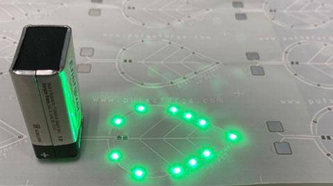
Chip components photonically soldered with SAC 305 alloy on PET flex
To see how this is possible, imagine pouring hot fudge on a scoop of ice cream. The fudge starts at a much higher temperature than the ice cream, but it can be added without melting the scoop. Why? Because melting the ice cream simply requires more heat than the fudge has to offer. And so, after a few seconds of thermal transfer throughout the dessert, you end up with fudge solidified on the surface of the ice cream, rather than a messy (but still delicious) puddle. It’s the subtle distinction between heat and temperature that makes the difference.

Back in the world of PCB assembly, this same distinction is what allows photonic soldering to process temperature-sensitive substrates without damage. With oven-based reflow, the solder alloy reaches its melting point along with the entire board, because temperature – not heat – is the control variable. By contrast, photonic soldering applies energy to the junction selectively, and the resulting molten solder dissipates its excess heat into the rest of the board as it cools. Much like hot fudge on frozen ice cream, solder reflowed with a PulseForge tool re-solidifies without melting the medium surrounding it. Temperature is important for photonic soldering, but heat is the control variable.
Of course, this explanation glosses over one crucial feature of photonic soldering: selectivity. So far, we have pointed out that the process confers a specific dosage of energy to just the solder joint, and not the substrate material. We will now explain why.
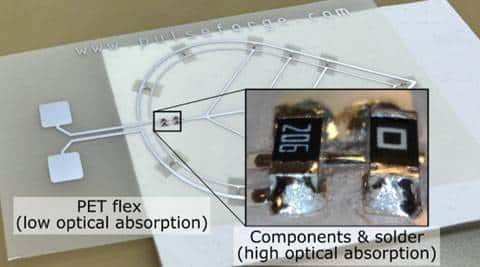
Here, the physical mechanism at work is optical absorption. Light absorbed by an object is converted to heat, since all energy is conserved. In this way, the rate of photonic heating is directly linked to optical absorptivity – that is, the fraction of incident light that is absorbed by a material, rather than reflecting back or passing through. When we look at an object, what we see is the visible light that leaves the object surface and eventually reaches our pupils. The higher an object’s optical absorptivity, the less light travels from the object to our retinas, and the darker that object appears in our vision.

Photonic soldering is still early in the development cycle. This means that research in the field possesses high impact potential for future implementation. Implementation of various devices on form materials has been the primary focus of both academic and industry researchers across a wide range of institutions. Studies are also ongoing to develop and understand form materials, solder alloys and junction quality toward full implementation of photonic soldering technology. PulseForge batch tools provide a robust and economical platform for researchers to get involved.
So, what does this mean for my application?
Circumventing the thermal limitations of temperature-sensitive substrates opens a new creative landscape for designers of electronic devices. Photonic soldering enables completely new combinations of functionality and form. Coupled with the lower cost of the final product, this processing approach is a winning formula for the next generation of electronics.
What can you come up with as we explore the possibilities?
*Please download PDF for references and citations.

Ara Parsekian, Ph.D.
Applications Engineer,
PulseForge Inc
Related PulseForge in Research
Published – 8/16/2022
Author – Ara Parsekian, Ph.D
Download as a PDF

There is a catch, however. Conventional PCB manufacturing requires solder reflow in a convection oven, and not all materials used in everyday objects can survive the oven environment. This is especially true for thermoplastic polymers – the plastic used in soft drink bottles, for example – which show up everywhere, due to their fantastic versatility and cost-effectiveness.
Conventional wisdom is that these materials can’t withstand the temperature required to reflow most solder alloys, and therefore, they can’t be used in circuits. When your board substrate melts at a lower temperature than your solder paste, you have a problem…or do you?

Chip components photonically soldered with SAC 305 alloy on PET flex

To see how this is possible, imagine pouring hot fudge on a scoop of ice cream. The fudge starts at a much higher temperature than the ice cream, but it can be added without melting the scoop. Why? Because melting the ice cream simply requires more heat than the fudge has to offer. And so, after a few seconds of thermal transfer throughout the dessert, you end up with fudge solidified on the surface of the ice cream, rather than a messy (but still delicious) puddle. It’s the subtle distinction between heat and temperature that makes the difference.
Back in the world of PCB assembly, this same distinction is what allows photonic soldering to process temperature-sensitive substrates without damage. With oven-based reflow, the solder alloy reaches its melting point along with the entire board, because temperature – not heat – is the control variable. By contrast, photonic soldering applies energy to the junction selectively, and the resulting molten solder dissipates its excess heat into the rest of the board as it cools. Much like hot fudge on frozen ice cream, solder reflowed with a PulseForge tool re-solidifies without melting the medium surrounding it. Temperature is important for photonic soldering, but heat is the control variable.
Of course, this explanation glosses over one crucial feature of photonic soldering: selectivity. So far, we have pointed out that the process confers a specific dosage of energy to just the solder joint, and not the substrate material. We will now explain why.
Here, the physical mechanism at work is optical absorption. Light absorbed by an object is converted to heat, since all energy is conserved. In this way, the rate of photonic heating is directly linked to optical absorptivity – that is, the fraction of incident light that is absorbed by a material, rather than reflecting back or passing through. When we look at an object, what we see is the visible light that leaves the object surface and eventually reaches our pupils. The higher an object’s optical absorptivity, the less light travels from the object to our retinas, and the darker that object appears in our vision.
This phenomenon is the reason that light-colored clothing is recommended for hot, sunny days. Darker clothing leads to faster heating than lighter clothing, even if the sun that provides the warmth is the same.


Photonic soldering is still early in the development cycle. This means that research in the field possesses high impact potential for future implementation. Implementation of various devices on form materials has been the primary focus of both academic and industry researchers across a wide range of institutions. Studies are also ongoing to develop and understand form materials, solder alloys and junction quality toward full implementation of photonic soldering technology. PulseForge batch tools provide a robust and economical platform for researchers to get involved.
So, what does this mean for my application?
Circumventing the thermal limitations of temperature-sensitive substrates opens a new creative landscape for designers of electronic devices. Photonic soldering enables completely new combinations of functionality and form. Coupled with the lower cost of the final product, this processing approach is a winning formula for the next generation of electronics.
What can you come up with as we explore the possibilities?
*Please download PDF for references and citations.

Ara Parsekian Ph.D.
Applications Engineer, PulseForge Inc